"/>
"/> "/>
"/>Additive manufacturing sheds new light on material structures at the ALBA Synchrotron

The ALBA Synchrotron is not your average research center: it’s one of the very few synchrotrons in the world. It is a large scientific infrastructure located in Cerdanyola del Vallès, Barcelona, that makes the powerful techniques of the ALBA Synchrotron available to researchers from both the academic community and the industrial sector, for them to carry out their own experiments. Since ALBA began operating in 2012, it has been hosting experiments from users mainly from Spanish institutions (65%), but also from other countries (35%).
The ALBA Synchrotron houses a complex of electron accelerators that generate synchrotron light. Once generated, this light is directed to the different laboratories, known as beamlines, where we can then visualize the atomic and molecular structure of materials and study their properties.
ALBA currently has eight operational beamlines using soft X-rays or hard X-rays, which are mainly intended to study materials and processes in a wide variety of scientific fields, such as life sciences and biosciences, batteries, catalysts, condensed matter (nanoscience and magnetic and electronic properties) and material science. Five more beamlines are now under construction. This large scientific infrastructure generates about 6,000 hours of light annually, and more than 2,000 researchers per year are benefiting from the intense X-rays generated at the ALBA Synchrotron.
The special needs of a facility such as ALBA arise from the great complexity in most of the pieces of each beamline. Each beamline has a specific structure and equipment, often tailor-made as it does not exist on the market, and a workstation where the experiments are carried out. As we host many different types of experiments, we find ourselves in constant need of being able to adapt each workstation to the requirements of each user of our facility. In the vast majority of cases, the experiment lasts a week at most, and the required tools and/or elements are rarely used again. Before 2016, all this adaptation was made with conventional subtractive technologies, and it took about 15 days to make the necessary parts. There was no margin for error and the cost was high. Since 2016, things have changed with the creation of the additive manufacturing service in ALBA.
Additive manufacturing is extremely useful as it reduces production costs, increases manufacturing speed, and pushes the limits of design. In our case, it has been very important, particularly in devices related to laboratory equipment, which is very expensive, and oftentimes the element we need is not always on the market. An example of an additively manufactured device is this one published in the following article from the CLAESS beamline, “Low-cost vacuum compatible liquid cell for hard X-ray spectroscopy” (Figure 1) (1*). Here, the efficiency of additive manufacturing is demonstrated through the creation of a liquid cell for X-ray absorption spectroscopy, compatible with absorption and fluorescence measurements.
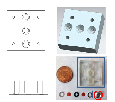
However, this is not the final design used for the beamline. The design needed to evolve in order for us to get the most out of it, which was done so by increasing the number of samples of the same cell. Therefore, instead of having only 3 metal cells per experiment, which limits the speed of sample analysis because of having to clean and replace the content of each cell, a new cell was designed to print about 20 cells per experiment. This way, the samples can be prepared the day before and, on the day of the experiment, the sample changing can be done more fluidly, turning the low-vacuum cells into a consumable.
The area in which ALBA stands out for its innovation is, in fact, not within printing; it undoubtedly lies in polymer research. As we have previously mentioned, one of the lines of work in our center is material science research. ALBA has several beamlines where material properties can be studied, but there are two where the properties of thermoplastics used for additive manufacturing are being investigated with some frequency: NCD-SWEET and MIRAS.
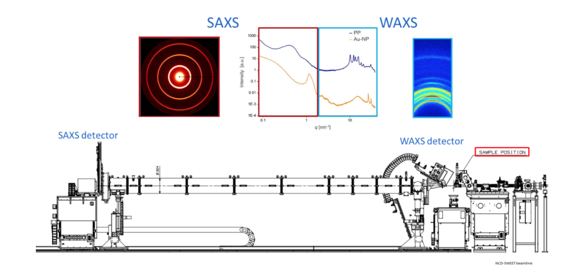
The Non-Crystalline Diffraction beamline, NCD-SWEET, uses two techniques to analyze the materials (Figure 2). The first one, Small Angle X-ray Scattering (SAXS) experiments, provides structural and dynamic information of large molecular assemblies like polymers, colloids, proteins, and fibers. A wide range of fields (medicine, biology, chemistry, physics, archaeological, environmental, and conservation sciences and materials) can be covered by this technique. SAXS is a very powerful technique that is used to study the supramolecular organization in biological systems, the structure and function of muscle filaments, corneal transparency, biological membranes, polymer processing, self-assembly of mesoscopic metal particles, colloids, inorganic aggregates, liquid crystals and devices. This powerful technique is combined with Wide Angle X-ray Scattering, WAXS, that provides the crystalline structure recording Bragg peaks.
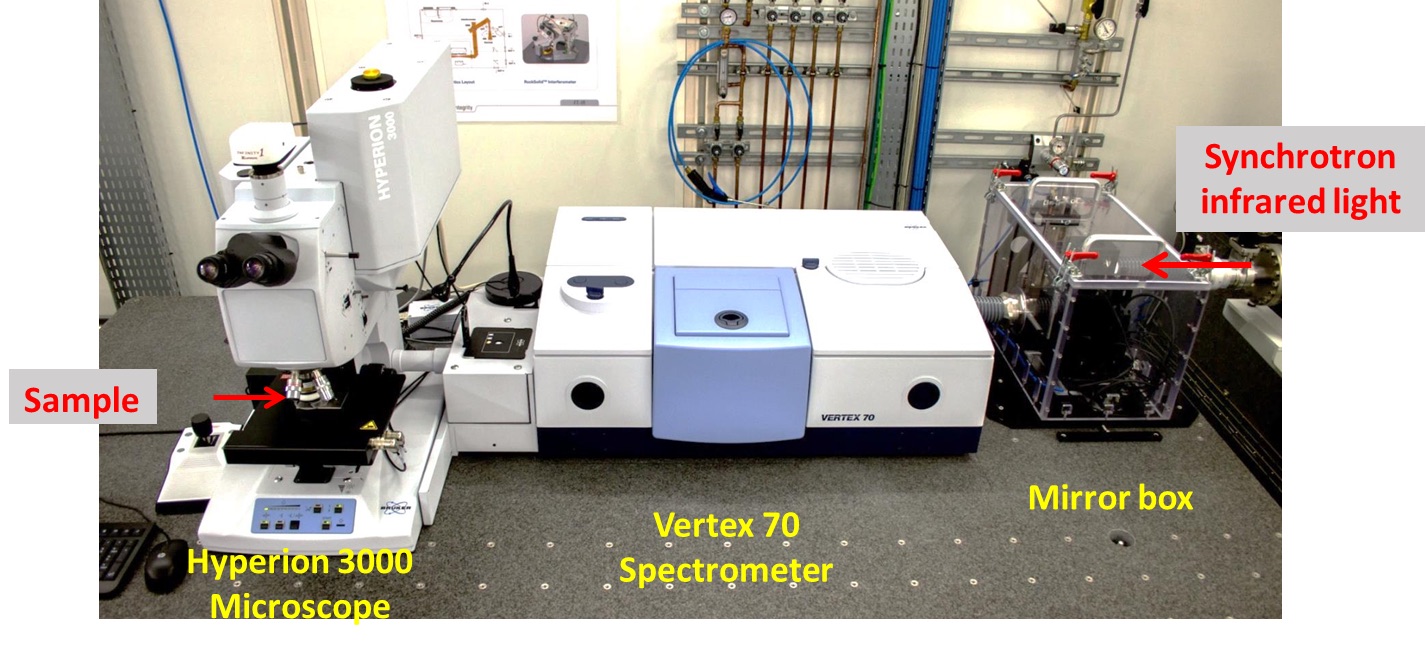
On the other hand, MIRAS is devoted to Fourier Transform Infrared (FTIR) spectroscopy and microscopy (Figure 3). FTIR is a very powerful tool to identify the vibrational signatures, and therefore the chemical composition of materials. The potential scientific applications of MIRAS cover a wide range of research fields, including materials science and their interfaces, biology and biomedicine, archaeology, geology, earth and space science, environmental science, extreme conditions, etc.![]()
Experiments performed at ALBA related to additive manufacturing
- Controlling the morphology of polymers (2*):
In this study, measurements were performed to determine the impact of materials and printing conditions on the morphology and properties of 3D printed objects. This is currently one of the key factors leveraging the performance and the quality of 3D printers.
This research intended to show how each step of the additive process can affect bulk, surface, and layer properties, and to present case studies regarding variations of morphology in filaments produced by Fused Deposition modeling, simply by varying processing parameters. (Figure 4).
- Structure development in polymers during fused filament fabrication:
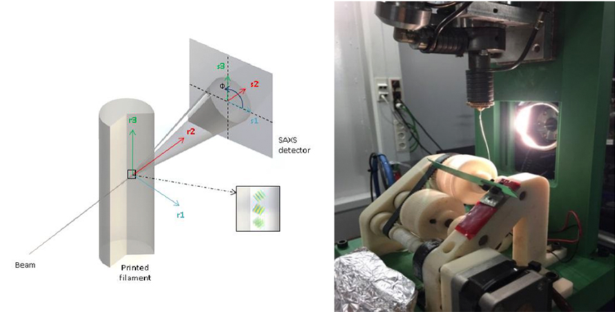
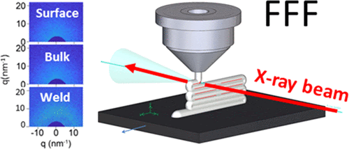
An in situ Small and Wide Angle X-ray Scattering Study (3*). Microstructure formation in individual layers during fused filament fabrication (FFF) of a Π-shaped multilayer single-walled polymer sample was studied by simultaneous measurement of small- and wide-angle X-ray scattering (SAXS and WAXS, respectively) methods employing synchrotron radiation.
The individual layers and the welding zone between them were investigated. As a model material, isotactic polypropylene (iPP), which is a commodity semicrystalline polymer with strong potential as a feedstock material for additive manufacturing, was used. The layers were deposited by an FFF three-dimensional (3D) printer that was custom-built to fit into the synchrotron beamline (Figure 5). WAXS data was utilized to determine the temperature of the irradiated volume. The polymer microstructure was characterized in terms of crystallinity and long-spacing.
Avrami analysis indicates that the crystallization behavior of iPP in thin layers is rather similar to that observed in quiescent crystallization of bulk iPP, suggesting similar nucleation and growth mechanisms. The results revealed a variation of crystallinity across the individual layers, reflecting the influence of interfaces (free surface and welding zone) on the final crystallinity of the thin layer (thickness h = 0.02 cm): the polymer is more crystalline in the bulk of the layer and less crystalline in the vicinity of the interfaces.
This effect can be advantageous to facilitate the welding between the layers i.e. to improve the overall mechanical performance of the 3D-printed object, because welding between layers is expected to occur by polymer chain interdiffusion. Along the thin layer, a higher crystallinity was observed near the corners attributed to a deceleration of the print head.
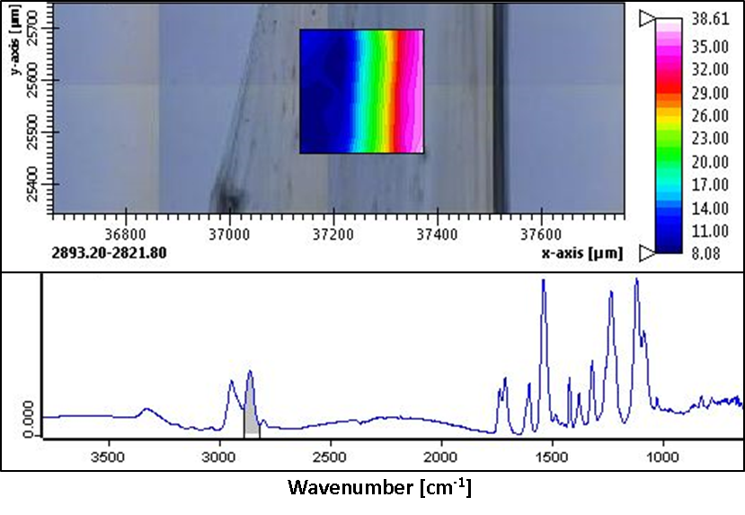
- Structural characterization of 3D printed polymer films by polarized infrared microspectroscopy:
Over the years, the performance of polymers has been constantly improved either by advances in their chemical design or by improvements in their processing. It is well documented that the processing conditions of semicrystalline polymers strongly influence their crystalline morphology and, thus, the final properties of the product. Fused filament fabrication (FFF) is one of the methods based on the continuous layer-by-layer deposition of a polymer melt produced by hot extrusion. Upon deposition, the polymer melt cools down and solidifies. If a semicrystalline polymer is employed, the solidification process of the extruded polymer may crystallize. A significant barrier to understanding this process is the lack of measurement techniques to quantify molecular orientation and crystallinity after polymer filament extrusion.
To address this issue, polarized FTIR microspectroscopy was used to measure the orientation of the polymer molecules and the crystallinity of the extruded films in the individual fibres and the welding zone between them. Thin film samples of commercially available polylactic acid (PLA), an insoluble, synthetic biodegradable polymer, are printed. The characterization of the 3D printed polymer thin films by polarized FTIR microspectroscopy allows correlating sample preparation parameters (printing temperature, sample design, and extruder size) with molecular orientation, crystallization, homogeneity, and elasticity of the samples. A first test performed at MIRAS showed the capability of using the 3D printers for polymer sample preparation.
Conclusion
All in all, additive manufacturing has become very important at the ALBA Synchrotron, providing the freedom to design specific laboratory equipment otherwise unavailable on the market. In turn, this new reach means that a variety of experiments can be conducted in order to continue researching and furthering additive manufacturing.
References
1* C. Marini, R. Boada, J. Prieto Burgos, N. Ramanan, I. García Domínguez, J. Zhao, T.T. Xiao, L. Simonelli, Low-cost vacuum compatible liquid cell for hard X-ray spectroscopy, Nuclear Inst. and Methods in Physics Research, A 908 (2018) 333–337
2* Ana O. Tojeira, Sara S. Biscaia, Tânia Q.Viana, Inês S. Sousa, Geoffrey R. Mitchell, Controlling the morphology of polymers in 3D Printing, Controlling the Morphology of Polymers pp 181-207
3* A. Nogales, E. Gutiérrez, M. C. García-Gutiérrez, T. A. Ezquerra, E. Rebollar, I. Šics, M. Malfois, S. Gaidukovs, K. Celms, G. Bakradze, Structure development in polymers during fused filament fabrication: An in situ Small and Wide Angle X-ray Scattering Study, Macromolecules 2019, 52, 24, 9715–9723